Developments of InGaN-based double hetero-structure high brightness blue LEDs and future lighting
Shuji Nakamura
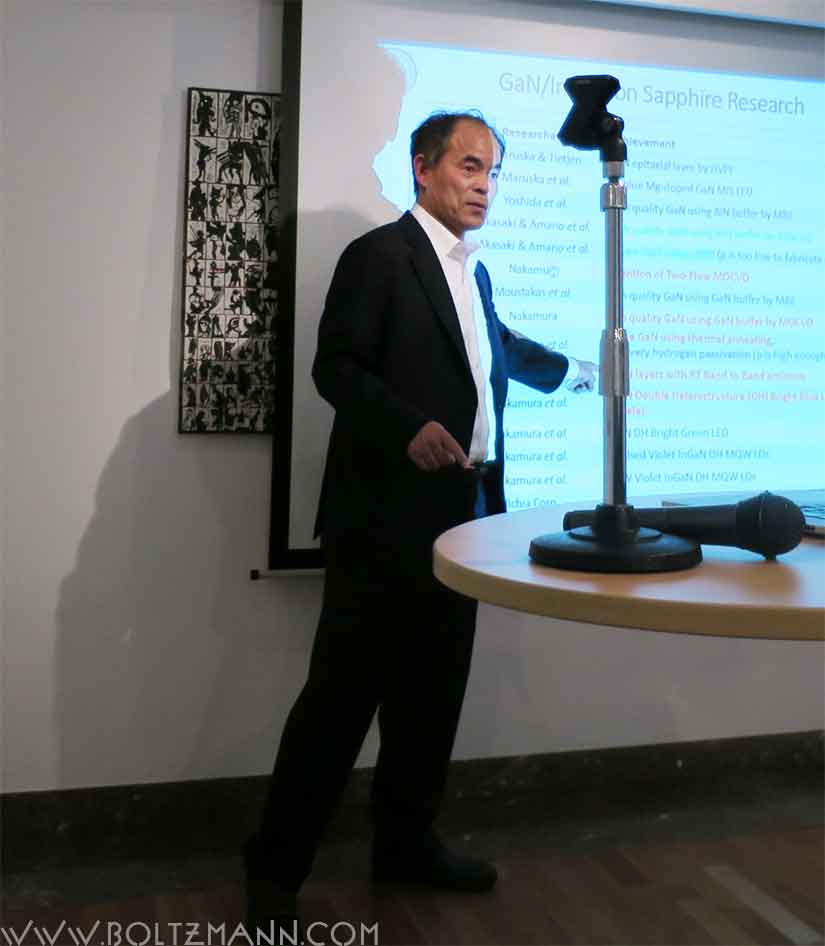
keynote talk given at the 7th Ludwig Boltzmann Forum, Austrian Embassy in Tokyo, 20th February 2015
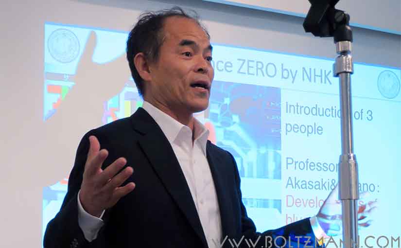
by Shuji Nakamura, Nobel Prize in Physics 2014. Inventor of blue GaN LEDs and lasers. Professor, Solid State Lighting and Energy Electronics Center, Materials and ECE Departments, University of California, Santa Barbara, USA
summary by Gerhard Fasol
Why Shuji Nakamura’s Nobel Prize is “for the invention of efficient blue light-emitting diodes which has enabled bright and energy-saving white light sources” and not for “development of mass production technology of blue LEDs”
The Royal Swedish Academy of Sciences awarded the Nobel Prize of Physics 2014 to Isamu Akasaki (1/3), Hiroshi Amano (1/3) and Shuji Nakamura (1/3), “for the invention of efficient blue light-emitting diodes which has enabled bright and energy-saving white light sources“
In an interview for the Japanese Mainichi-Shinbun, the Chairman of the Nobel Prize Committee in Physics, Professor Per Delsing summarized the key discoveries of each Nobel Laureate from the point of view of the Nobel Prize Committee in Physics:
- Isamu Akasaki: High quality GaN with AlN buffer
- Hiroshi Amano: Demonstration of GaN pn junction
- Shuji Nakamura: Many contributions to achieve a practical level of high efficient blue LEDs
The discovery of blue GaN LEDs is a discovery in the field of Physics achieved by three people, their contributions are:
- Isamu Akasaki and Hiroshi Amano
- AlN buffer (to grow AlN of sufficient quality on a substrate of a different material)
- p-GaN by electron beam irradiation
- realization of GaN pn junction
- Shuji Nakamura
- GaN buffer (to grow GaN of sufficient quality on a substrate of a different material)
- p-GaN by thermal annealing and the theoretical clarification of the mechanism for p-type conductivity
- the invention of InGaN-based high brightness double-heterostructure blue LEDs (the Nobel Prize was given to the invention of this LED)
Nobel Prizes are not awarded for the development of “mass manufacturing technologies”…
Alfred Nobel’s will reads:
“The whole of my remaining realizable estate shall be dealt with in the following way: the capital, invested in safe securities by my executors, shall constitute a fund, the interest on which shall be annually distributed in the form of prizes to those who, during the preceding year, shall have conferred the greatest benefit on mankind. The said interest shall be divided into five equal parts, which shall be apportioned as follows: one part to the person who shall have made the most important discovery or invention within the field of physics;…”
It is perfectly clear in Alfred Nobel’s will, the Nobel Prize Committee awards Nobel Prizes in Physics for “the most important discoveries or inventions within the field of physics” – not for the development of manufacturing technologies.
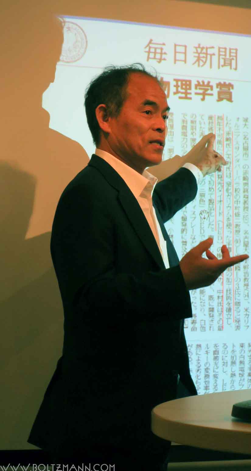
Shuji Nakamura explained these facts on numerous occasions to Japanese media, and also today at the 7th Ludwig Boltzmann Forum. It is difficult to understand why Japanese media and Government organizations did not take this information in.
It is a mystery why Japan’s National Television NHK, several Japanese major newspapers, The Journal of the Japanese Society of Applied Physics, Japan’s New Energy and Industrial Technology Development Organization (NEDO), Japan’s Science Technology Agency JST and several other Japanese organizations insist that the Nobel Prize should have been awarded as follows:
- Professors Akasaki and Amano for the development of the blue LED
- Professor Nakamura for the development of manufacturing technology – although it is clear that the Nobel Prize is only awarded for profound discoveries and inventions in the field of physics and not for the development of manufacturing technologies
Clearly there is a disconnect between these major Japanese media organizations, two major Japanese Government Research Organizations NEDO and JST and reality regarding the reason why Shuji Nakamura was awarded the Nobel Prize in Physics 2014.
Metal-Insulator-Semiconductor (MIS) devices vs pn-Junction vs Double Heterostructure (DH) light emitting diodes (LED):
Metal-Insulator-Semiconductor (MIS) devices achieve relatively low intensity, weak light emission at the metal / insulator / n-type or p-type semiconductor interface, thus only n-type or p-type doping is necessary. In the case of GaN, n-type GaN was first demonstrated by Maruska in 1973 (H. P. Maruska, D. A. Stevenson, J. I. Pankove, Appl. Phys. Lett., 22 (1973) p 303-305. In these MIS GaN LEDs visible violet electroluminscence was observed, however it was too dim for practical applications, and the necessary voltage was too high for practical application – 15 Volt.
p-type GaN and InGaN was demonstrated by Akasaki and Amano with electron beam annealing, and the real breakthrough was by Shuji Nakamura by annealing in Nitrogen gas.
On October 20, 1993, the Japanese Journal Nikkan Kogyo announced that “MIS type blue LEDs with a brightness of 200mCd were developed by Toyoda Gosei Co Ltd through industry-University cooperation funded by Japan’s Science and Technology Agency (JST). However, both the MIS LEDs demonstrated by Maruska et al in 1973, and those introduced by Toyoda Gosei in 1993 were too weak for real applications.
Another intermediate step in development are p-n junction LEDs, without double heterostructure. Such LEDs also have relatively low light efficiency, since electrons and holes have small overlap and therefore low recombination probability. The quantum confinement of electrons and holes in the same location in space is necessary to achieve high recombination efficiency and thus high brightness.
For high brightness GaN LEDs it was necessary to develop viable n-type / p-type InGaN heterostructure LEDs. This was done by Shuji Nakamura, and for example announced by the Japanese Journal Nikkei Sangyo on November 1993: “p-n junction InGaN double heterostructure (DH) LEDs with a brightness of more then 1000 mCd were developed by Nichia Chemical Industries Ltd”, when Shuji Nakamura was at Nichia from 1979-1999. It is for the invention and development of these LEDs that Shuji Nakamura was awarded the Nobel Prize.
Shuji Nakamura delivered his Nobel Lecture on 8 December 2014, at Aula Magna, Stockholm University:
- Interview with the Chairman of the Nobel Prize Committee in Physics, Professor Per Delsing:
Interview about the 2014 Nobel Prize in Physics (6 minutes) - Introduction by Professor Per Delsing, Chairman of the Nobel Committee for Physics.
- Nobel Lecture by Shuji Nakamura (26 minutes)
- http://www.nobelprize.org/nobel_prizes/physics/laureates/2014/nakamura-lecture-slides.pdf
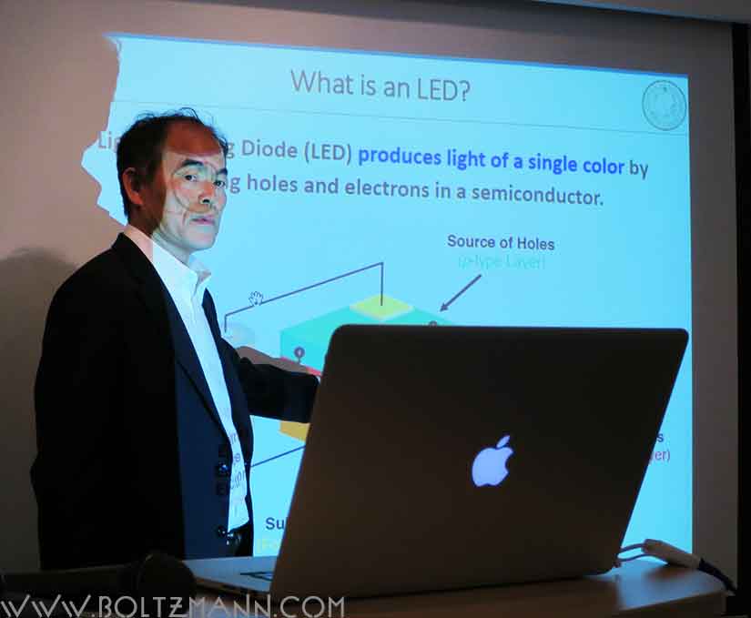
1. Introduction: What is an LED?
Light emitting diodes (LED) produce light of a single color, in a narrow frequency interval (e.g. red, yellow, blue, green) by combining holes and electrons in a semiconductor.
To produce white light needed for lighting, either LEDs of different color can be combined, or blue light can be converted into white light using yellow phosphor.
Applications for InGaN-based LEDs include:
- solid state lighting, replacing light bulbs and fluorescent tubes (and fire in developing countries, or emergencies)
- decorative lighting
- automotive lighting
- displays (e.g. flat panel displays for mobile phones, PCs, TVs)
- agriculture
- indoor lighting
Energy savings impact – for the USA alone:
Approx. 40% electricity savings (261 TeraWatthours) in USA in 2030 due to LEDs.
InGaN LEDs eliminate the need for 30++ 1000MW power plants by 2030.
InGaN LEDs avoid generating about 185 million tons of CO2.
Light efficiency:
- oil lamp (15,000BC): 0.1 lm/W
- light bulb (19th century): 16 lm/W
- fluorescent lamp (20th century): 70 lm/W
- LED (21st century): 300 lm/W
2. Material of choice: ZnSe vs GaN
Both ZnSe (II-VI compounds) and GaN (III-V compounds) have the electronic band gap and other properties to efficiently generate blue light. In 1989 the situation was:
- ZnSe can be grown on GaAs substrates with 0% lattice mismatch and few dislocations.
- high crystal quality: dislocation density < 1 x 10^3 cm^-2
- very active research in 1989: > 99% of researchers on blue LEDs
- interest at 1992 JSAP Conference: 500 people audience
- GaN grown on Sapphire (Al2O3) has a 16% lattice mismatch leading to a high defect (dislocation) density.
- Poor crystal quality: dislocation density > 1 x 10^9 cm^-2
- little research in 1989: < 1% of researchers on blue LEDs
- interest at 1992 JSAP Conference: < 10 people audience
- GaN research was actively discouraged: “GaN has no future”, “GaN people have to move to ZnSe material”….
1989 was the starting point of Shuji Nakamura’s research. Based on his experience at University of Miami, Shuji Nakamura wanted to achieve a PhD degree by writing research papers. The GaN field had the advantage that there were very few researchers and papers, so it was a great topic to publish lots of papers! Working at a small company the budget was small, and there was only one researcher: Shuji Nakamura.
It was commonly accepted in the 19970s-1980s, that LEDs need dislocation density < 1 x 10^3 cm^-2. Shuji Nakamura never thought at that time that he could invent blue LEDs using GaN….
3. The beginning: GaN on Sapphire
Before the 1990s, GaN was grown using conventional MOCVD systems, as described for example in H. Amano, N. Sawaki, I. Akasaki, Y. Toyoda, Appl. Phys. Lett. 48 (1986), 353-355.
Conventional MOCVD systems have high carrier gas velocity (about 4.25 m/s), poor uniformity, poor scalability, poor reproducibility, poor control. An AlN buffer layer was introduced to create crack free GaN growth, however, Al causes significant problems in the MOCVD reactor.
Shuji Nakamura’s most significant invention: two-flow MOCVD
To overcome the problems of conventional MOCVD, Shuji Nakamura invented “two-flow MOCVD” where a second “subflow” vertical to the surface of the substrate gently “pushes” the gases down onto the substrate and improves the thermal boundary layer: S. Nakamura et al, Appl. Phys. Lett. 58 (1991) 2012-2023.
Two-flow MOCVD enables the reproducible growth of uniform, high quality GaN. Shuji Nakamura told us, that two-flow MOCVD was his most important invention.
With this new two-flow MOCVD method, Shuji Nakamura grew the first MOCVD GaN buffer layers on 2″ Sapphire substrates, and achieved the highest Hall mobilities reported at that time: S. Nakamura, Jpn. J. Appl. Phys. 30 (1991) L1705-L1707.
Overcoming passivation of p-type GaN
Shuji Nakamura discovered that hydrogen ions (H+) from dissociation of ammonia (NH3) contained in the growth gases is the source of passivation of p-type GaN which prevented the growth of p-type GaN, see:
S. Nakamura et al., Jpn. J. Appl. Phys. 31 (1992) L139-L142, and
S. Nakamura et al., Jpn. J. Appl. Phys. 31 (1992) 1258-1266.
Thermal annealing in hydrogen ion free atmosphere overcomes passivation
Previously all researchers used an atmosphere containing H+ to anneal p-type GaN, which was passivated by this process. Shuji Nakamura discovered that it was necessary to anneal in a H+ free atmosphere to achieve p-type GaN.
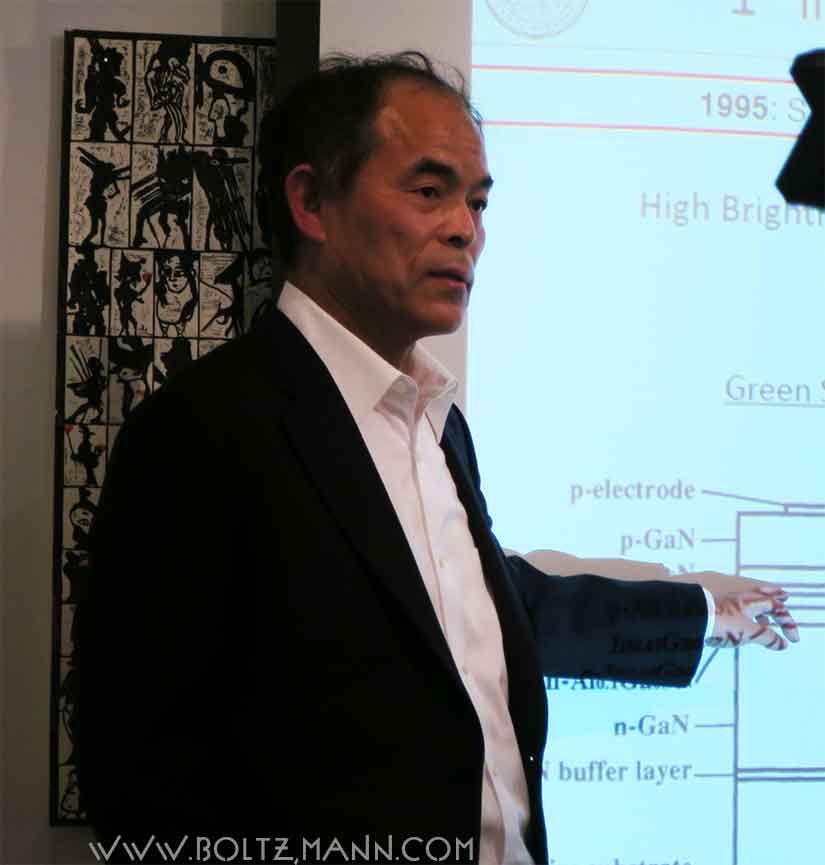
From p-n GaN homojunctions to InGaN double heterostructures (DH)
Akasaki and Amano developed p-n GaN homojunctions. These have good crystal quality, but very dim light emission, are very inefficient, power output is below mW, and the emission is around 360nm in the Ultra-Violet (UV). These structures are not suitable for practical LEDs.
To overcome these difficulties, double heterostructure are necessary, which were invented by Z. I. Alferov and H. Kroemer, who were awarded the 2000 Nobel Prize in Physics.
Double heterostructures (DH) create a quantum well, were electrons and holes are confined, high carrier concentrations are achieved and the radiative recombination rates are enhanced.
4. Enabling the LED: InGaN
GaN heterojunctions are constructed by growing a sandwich structure consisting of n-GaN, InGaN, p-GaN. The band gap / color is adjusted by adjusting the Indium concentration in InxGa1-xN alloy. However this presents difficult challenges:
- It is hard to incorporate Indium, because of its high vapor pressure, Indium tends to boil off. Growth at lower temperatures to prevent Indium boil-off results in poor crystal quality
- It is necessary to grow very thin layers to build quantum wells. Growing very thin layers requires very fine control over the growth conditions and high interface quality.
- Indium introduces strain in the crystal because Indium is about 20% bigger than Gallium.
Because of these difficulties, research in the 1970s-1980s could not achieve InGaN of sufficiently high quality for room temperature band-to-band emission.
Shuji Nakamura’s two-flow MOCVD method succeeded to grow high quality InGaN with band-to-band emission and with controllable Indium concentration, so that the growth of InGaN with different band-gap and therefore controllable color spectrum became possible: S. Nakamura et al Jpn. J. Appl. Phys. 31 (1992) L1457-L1459.
With this breakthrough, Shuji Nakamura succeeded to grow the first high brightness InGaN LEDs: S. Nakamura et al, Appl. Phys. Lett. 54 (1994) 1687-1689.
Shuji Nakamura could grow the first InGaN quantum well blue, green and yellow LEDs using these methods: S. Nakamura et. al. Jpn. J. Appl. Phys. 34 (1995) L797-L799 and the first violet InGaN Multi-quantum-well laser diode: S. Nakamura et. al. Jpn. J. Appl. Physics 35 (1996) L74-L76.
InGaN LEDs are far less sensitive to defect density than other materials such as GaAs, GaP or GaN,
Lester et al, Appl. Phys. Lett. 66 (1995) 1249,
Chichibu, Nakamura et al. Appl. Phys. Lett. 69 (1996) 4188,
Nakamura, Science, 281 (1998) 956.
5. Historical perspective
While red GaAs/GaAsP LEDs where invented in the 1970s, progress in luminous efficiency of GaN and InGaN based green and blue LEDs, invented around 1992-1993 by Shuji Nakamura, is much faster. Today white LEDs far exceed light bulbs and fluorescent lamps in luminous efficiency.
USC’s vision: LED based white light is great, laser based white light is even better!
- LEDs: equivalent of a 60W light requires 28mm^2 chip, and external quantum efficiency peaks around 70% rapidly decreases with increasing current density beyond 0.1 kA/cm^2
- Lasers: equivalent of a 60W light requires 0.3mm^2 chip, and external quantum efficiency remains around 70% up to current densities of 2 kA/cm^2
References
- Shuji Nakamura, Nobel Prize in Physics 2014 Facts.
- Shuji Nakamura, Nobel Prize Lecture
- Shuji Nakamura, Stephen Pearton, Gerhard Fasol, “The blue laser diode”, Springer Verlag, 2nd edition
buy direct from Springer-Verlag (paper, and e-book version available), or
via Amazon.com

Copyright (c) 2015 Eurotechnology Japan KK All Rights Reserved