Shuji Nakamura, Nobel Prize in Physics 2014, Professor, University of California, Santa Barbara and Co-founder of Soraa
Shuji Nakamura: bottom-up innovation, not top-down innovation.
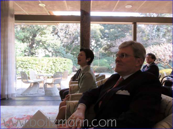
keynote talk given at the 8th Ludwig Boltzmann Forum at the Embassy of Austria, Tokyo, Thursday 18 February 2016
(summary of Shuji Nakamura’s talk – including some comments – by Gerhard Fasol)

by Shuji Nakamura, Nobel Prize in Physics 2014, Professor, University of California, Santa Barbara and Co-founder of Soraa
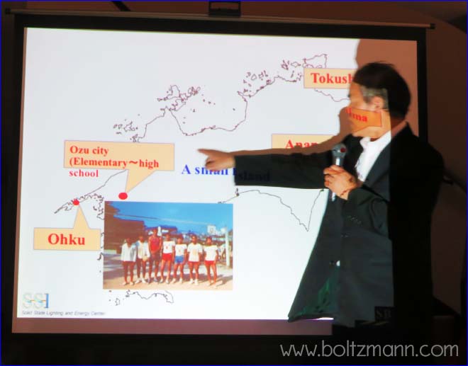
Shuji Nakamura is born on 22 May 1954 in Ohku, part of the village Yotsuhamamura (四ツ浜村, 4290 inhabitants) (日本 愛媛県西宇和郡四ツ浜村大久) on the Western side of Shikoku Island (四国, 4.2 million inhabitants), went to Elementary School and High School in Ozu (大洲), not far away, also on the Western side of Shikoku, studied at Tokushima University, which at that time did not have a Physics Department (Shuji Nakamura later won the Nobel Prize in Physics!), and then entered Nichia Chemical Industries in 1979 after graduating from the University of Tokushima. Nichia Chemical Industries is located in Anan, about 20 km south of Tokushima.
Until moving to the University of California in Santa Barbara, Shuji Nakamura spent his whole life, education, University, and professional work as researcher at Nichia entirely on the Island of Shikoku, with no connection to Tokyo, to Government, or Japan’s establishment, or research establishment.
Shuji Nakamura’s lack of connections to Japan’s establishment, industrial establishment, academic establishment or government establishment maybe at the origin of the many misunderstandings which have developed between Shuji Nakamura and Japan’s media, and some of Japan’s establishment.
Thus Shuji Nakamura is the perfect example of bottom-up innovation. Not planned from the top. Therefore maybe its hard for people at the top to grasp and accept.
Shuji Nakamura and his inventions have huge impact on the world, it is hard for Government and main stream media to accept, that Shuji Nakamura does not fit at all into planned top-down innovation, but has created his own independent path.
The contrast between Shuji Nakamura’s bottom-up innovation – recognized and rewarded by the Nobel Prize in Physics – and the official views of top-down innovation seems to have led to many misunderstandings. Shuji Nakamura is making much effort, including today’s talk at the 8th Ludwig Boltzmann Forum, to clear up these misunderstandings.
Invention of efficient blue light-emitting diodes vs. development of manufacturing technologies
The Royal Swedish Academy of Sciences awarded the Nobel Prize of Physics 2014 to Isamu Akasaki (1/3), Hiroshi Amano (1/3) and Shuji Nakamura (1/3), “for the invention of efficient blue light-emitting diodes which has enabled bright and energy-saving white light sources“.
In an interview for the Japanese Mainichi-Shinbun, the Chairman of the Nobel Prize Committee in Physics, Professor Per Delsing summarized the key discoveries of each Nobel Laureate from the point of view of the Nobel Prize Committee in Physics:
- Isamu Akasaki: High quality GaN with AlN buffer
- Hiroshi Amano: Demonstration of GaN pn junction
- Shuji Nakamura: Many contributions to achieve a practical level of high efficient blue LEDs
The discovery of blue GaN LEDs is a discovery in the field of Physics achieved by three people, their contributions are:
- Isamu Akasaki and Hiroshi Amano
- AlN buffer (to grow AlN of sufficient quality on a substrate of a different material)
- p-GaN by electron beam irradiation
- realization of GaN pn homo-junction
- Shuji Nakamura
- GaN buffer (to grow GaN of sufficient quality on a substrate of a different material)
- p-GaN by thermal annealing and the theoretical clarification of the mechanism for p-type conductivity
- the invention of InGaN-based high brightness double-heterostructure blue LEDs (the Nobel Prize was given to the invention of this LED)
The Nobel Prize Committee awarded the Nobel Prize to Shuji Nakamura for many contributions and inventions to achieve a practical level of high efficient blue LEDs
In his will, Alfred Nobel writes:
“The whole of my remaining realizable estate shall be dealt with in the following way: the capital, invested in safe securities by my executors, shall constitute a fund, the interest on which shall be annually distributed in the form of prizes to those who, during the preceding year, shall have conferred the greatest benefit on mankind. The said interest shall be divided into five equal parts, which shall be apportioned as follows: one part to the person who shall have made the most important discovery or invention within the field of physics;…”
It is perfectly clear from Alfred Nobel’s will, the Nobel Prize Committee awards Nobel Prizes in Physics for “the most important discoveries or inventions within the field of physics” – not for the development of manufacturing technologies.
Why is it that Japan’s major Government Organizations and media present a narrative of the LED invention which is opposite to the views of the Nobel Prize Committee and the scientific community outside Japan?
Shuji Nakamura expresses his frustration that the clear explanations of the Nobel Prize Committee’s reasons are not understood by Japanese Media, and many others.
It appears to Shuji Nakamura that there seems to be a widespread misunderstanding of who invented what, and who was awarded the Nobel Prize for what.
Japanese media (Yomiuri Shinbun and others), NHK (e.g. in the Science ZERO program), Japan’s New Energy and Industrial Technology Development Organization NEDO in their publications, Japan’s Science and Technology Agency JST, Japan’s Science Council JSC, Japan’s Ministry of Education, Culture, Sports, Science and Technology, all present a picture of the LED inventions which is opposite to the clear statements by the Nobel Prize Committee.
They all write that Professor Akasaka and Amano developed the blue LED in 1989 at Nagoya University, while Shuji Nakamura developed the manufacturing technology in 1993. Such a narrative fits well with a top-down picture, where Professors at Nagoya University make the scientific breakthrough, which is then transferred to industry, where an industrial researcher develops the manufacturing applications, which then the company commercializes.
This top-down narrative would fit well the top-down view of innovation, however this is not how the breakthrough invention of GaN LEDs and lasers, which are now leading to the global lighting revolution actually happened.
Shuji Nakamura explains the essential steps leading to the invention and development of high intensity GaN LEDs
Professor Akasaka and Amano developed homo-junction LEDs, which are very inefficient and show very dim light emission
Professors Akasaki and Amano developed methods to produced n-type and p-type GaN and grew homo-junction GaN LEDs, which emit light, but which are highly inefficient, and the light emission is very dim. Still, this discovery was a crucial step forward, and Akasaka and Amano were awarded shares of the Nobel Prize for these important developments.
For tunable colors, high output power an efficient device structure, and many other developments were necessary, which Shuji Nakamura achieved.
A crucial step forward was the development of heterostructure LEDs, where electrons and holes are confined in quantum wells formed by hetero-junctions, yielding higher efficiencies. Double heterostructures were invented by Z I Alferov and H Kroemer, who were awarded shares of the 2000 Nobel Prize in Physics for these and other inventions.
A series of inventions led to efficient blue LEDs:
- p-type GaN activated by electron beam irradiation (Akasaki & Amano, 1989)
- AlN buffer (Akasaki & Amano, 1985)
- GaN buffer (Nakamura, 1991)
- InGaN emitting active layer (Nakamura and Mukai, 1992)
- p-type GaN activated by thermal annealing. Hydrogen passivation was clarified as the origin of hole compensation (Nakamura at al, 1992)
Shuji Nakamura’s development of hydrogen free annealing of p-type GaN and the development of InGaN heterostructure lead to the breakthrough development of high brightness InGaN LEDs for blue emission
A particularly important discovery by Shuji Nakamura in 1992 was to find out why p-type GaN could not be efficiently produced previous to this invention. Shuji Nakamura found out that previous researchers had all annealed p-type GaN in hydrogen (H+) atmosphere, which passivated the p-GaN, making it useless for electronic devices.
Shuji Nakamura invented the method to anneal p-type GaN in a hydrogen-free atmosphere which for the first time allowed the production of proper p-type GaN layers.
This in 1994, Shuji Nakamura could report the first high brightness InGaN LEDs for blue emission, S. Nakamura et al, Appl. Phys. Lett. 64, (1994) 1687-1689.
It is a misunderstanding to emphasize only Shuji Nakamura’s developments of manufacturing technologies, and to forget about Shuji Nakamura’s many inventions in the field of physics for which he was awarded his share in the Nobel Prize in Physics
Had Shuji Nakamura developed “only” manufacturing techniques, Shuji Nakamura would certainly not have been awarded the Nobel Prize in Physics. Shuji Nakamura was awarded the Nobel Prize in Physics for a long string of discoveries and developments in the field of physics, in addition to developing a wide range of manufacturing technologies as well, such as the two-flow MOCVD equipment.
What is an LED? How to produce energy efficient white light?
A light emitting diode (LED) produces light of a single color corresponding to the energy difference of electrons and holes recombining across the bandgap in a semiconductor LED device.
By choosing different materials, LEDs emitting light of different colors can be produced. To produce white light, the light emitted by several different LEDs of different color can be combined, e.g. blue + yellow, or blue + yellow + red.
Another option to produce white light is to coat a blue light emitting LED with phosphor, where the phosphor converts part of the blue light into yellow light. The remaining blue light combined with the yellow light emitted by the phosphor appears white to the human eye.
Conventional white LEDs, consisting of blue LEDs covered by phosphor, show strong blue light emission, and disrupt the human circadian cycle and possibly suppresses melatonin (see: Narusawa et al, J. Phys. D: Appl. Phys. 43 (2010) 354002).
Most PCs, laptop, smartphone and tablet liquid crystal displays use such white LEDs for the background lighting, cause eye fatigue, and thus filters can be used to cut the blue light.
Apple has acknowledged the dangers of strong blue light emission, and has developed methods to reduce blue light emission. The blue “spike” in the white light output from electronic devices can reduced the production of the sleep inducing melatonin hormone, and has been linked to health disorders and even cancer.
What is an LED? How to produce energy efficient white light?
Applications for InGaN based LEDs:
- solid state lighting
- decorative lighting
- automobile lighting
- displays (e.g. for PCs, TV, tablets, smartphones
- agriculture:
- plant factories using blue/red LEDs in a clean room achieves growth rates 2.5 – 5 times higher than in nature
- achieve 50%-90% higher yields
- water consumption 1% compared to outside
- indoor lighting
Energy savings impact: save 60 nuclear power stations globally until 2020
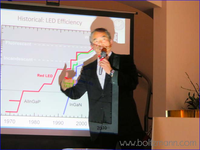
LEDs are 4 times as energy efficient as fluorescent tubes, and about 20 times as efficient as incandescent bulbs:
- oil lamp: 0.1 lumen/Watt
- incandescent light bulb: 16 lumen/Watt
- fluorescent lamp: 70 lumen/Watt
- LED lamp: 300 lumen/Watt
Converting traditional lighting to LED lighting, we can reduce global energy consumption corresponding by an amount corresponding to 60 nuclear power stations by 2020:
- Japan could save 7 nuclear power plants by converting lighting to LEDs
- Germany could save 3 nuclear power plants
- USA could save 19 nuclear power plants
- China could save 17 nuclear power plants
- India could save 9 nuclear power plants
Nichia vs Nakamura lawsuits
Time line:
- 1993 Nakamura et al: first high efficiency blue InGaN LED was invented, Nobel Prize in Physics
- 1995 Nakamura et al: first violet InGaN laser diode was invented
- 1999 Nichia Chemical Industries: first products of violet InGaN laser diode
- 2000 Shuji Nakamura quits Nichia Chemical Industries and moves to University of California Santa Barbara
- 2000 Nichia Chemical Industries starts the lawsuit against Nakamura alleging infringements of trade secrets in USA
- 2001 Nakamura starts the counter lawsuit against Nichia Chemical Industries using the patent law article No. 35
- 2002 Nakamura wins the lawsuit regarding trade secrets in the USA against Nichia
- 2004 Nakamura wins wins US$ 200 million against Nichia as a reasonable compensation fee at Tokyo District Court
- 2005 Nakamura settlement by winning US$ 8 million with Nichia as a reasonable compensation fee at Tokyo High Court
- 2014 Nakamura wins Nobel Prize in Physics
Japan’s vs US judicial system – Shuji Nakamura’s experiences
- No discovery process in Japan: no need to submit documents or evidence, no depositions
- No discussions at court hearing; both lawyers submit statements and prepared documents to the judge without discussion
- Ruling: ruling determined by how many people could benefit by ruling
- Penalties: penalties are determined by precedence and earlier rulings. Punishments and penalties are generally much higher in the USA, thus much higher sanctions for breaking the laws
- Judges’ salaries in Japan are determined by superiors, while in the USA the salary of each judge is guaranteed by the constitution
- IP lawsuits tend to move to the USA, because USA includes discovery process and higher awards for the winners of lawsuits
- No perjury in Japan. Harder to enforce truth of parties statements in Japan.
- Libel or defamation are weakly sanctioned, fines/awards are relatively low and on the order of US$ 10,000 in Japan.
Key elements for success
- risk taking
- innovation and flexibility
- team diversity
- intellectual freedom – thinking differently
- hard work
- infrastructure and cultural support for innovation or failure
More information
- Shuji Nakamura’s website at the University of California, Santa Barbara
- Soraa
- Shuji Nakamura: Developments of InGaN-based double hetero-structure high brightness blue LEDs and future lighting, 7th Ludwig Boltzmann Forum, 20 February 2015
- Nobel Prize 2014, Shuji Nakamura, Facts
- Shuji Nakamura, Gerhard Fasol, Stephen J Pearton: The Blue Laser Diode: The Complete Story, 2nd Edition, Springer Verlag 2000
Copyright (c) 2016 Eurotechnology Japan KK All Rights Reserved